
Introduction
FPGA Statistics: FPGAs (Field-Programmable Gate Arrays) are reconfigurable integrated circuits with programmable logic blocks and interconnects, allowing custom digital hardware designs to be created and modified after manufacturing, offering parallel processing, low latency, and flexibility for applications in telecommunications, aerospace, and high-performance computing, with key elements including CLBs, BRAM, DSP blocks, and I/O, differing from CPUs by performing operations in parallel rather than sequentially, and often used for prototyping or low-volume production.
Field-programmable Gate Arrays, commonly referred to as FPGAs, are semiconductor devices that offer flexible and modifiable hardware functionalities. They consist of multiple reconfigurable logic blocks and programmable interconnections, enabling users to design and implement customised digital circuits without the necessity of fabricating their own specific silicon.
FPGAs find applications in various industries, including telecommunications, aerospace, and industrial automation, where rapid development, reduced latency, and powerful processing capabilities are essential. Their versatility makes them an invaluable resource for hardware innovation, research, and specialised computing tasks.
Editor’s Choice
- The Global Field-Programmable Gate Array (FPGA) market is set for consistent growth in the upcoming years, with a compound annual growth rate (CAGR) of 7.8%.
- According to the most recent data, SRAM-based FPGAs lead the market, holding a 39% market share.
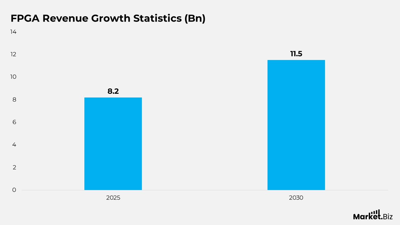
- The overall market revenue was recorded at $6.5 billion.
- System-on-Chip Field-Programmable Gate Arrays (SoC FPGAs) provide a range of processing capabilities that are customised for various applications.
- FPGAs also excel in performing multiplication operations directly in hardware, a characteristic appreciated by 24% of those surveyed.
General FPGA Statistics
- The Global Field-Programmable Gate Array (FPGA) market is set for consistent growth in the upcoming years, with a compound annual growth rate (CAGR) of 7.8%.
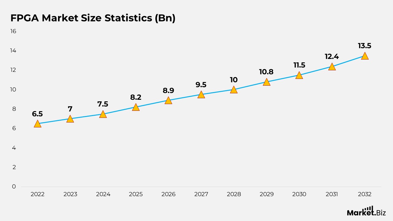
- In 2022, the revenue generated by the FPGA market was USD 6.5 billion, and it is projected to rise to USD 13.5 billion by 2032.
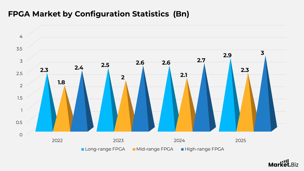
- In 2022, the contribution from low-range FPGAs amounted to USD 2.3 billion, while mid-range FPGAs accounted for USD 1.8 billion, and high-range FPGAs generated USD 2.4 billion.
- According to the most recent data, SRAM-based FPGAs lead the market, holding a 39% market share.
- Resistance (R) in the switch and parasitic capacitance (C) are crucial factors influencing signal propagation.
- ONO anti-fuse FPGAs exhibit moderate resistance (300-500 ohms) and low capacitance (5F), whereas amorphous anti-fuse FPGAs show lower resistance (50-100 ohms) and slightly elevated capacitance (1.1-1.3F).
- The FPGA segment and a hard processor system (HPS) centered on a single or dual-core 32-bit Arm Cortex-A9 MPCORE functioning at 925 MHz.
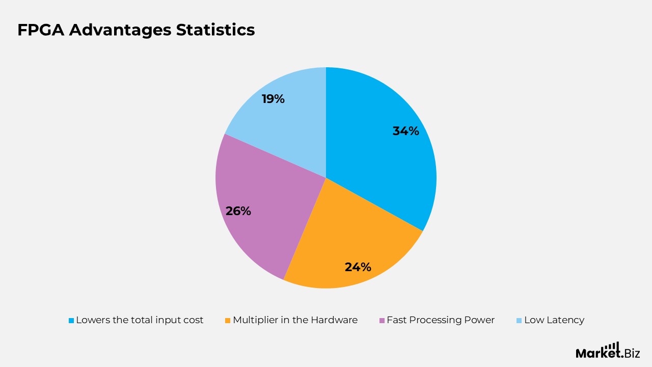
- 34% of surveyed individuals recognise the ability of FPGAs to reduce the overall input cost, rendering them a cost-efficient option for a variety of applications.
FPGA Market Size Statistics
- In 2022, the revenue of the FPGA market was recorded at USD 6.5 billion, with an anticipated rise to USD 7 billion in 2023.
- The upward trend continues, with projected revenues of USD 7.5 billion in 2024, USD 8.2 billion in 2025, and USD 8.9 billion in 2026.
- Looking ahead, the market is expected to achieve USD 9.6 billion in 2027, USD 10.0 billion in 2028, and USD 10.8 billion in 2029.
- The growth trajectory is expected to continue, with revenues estimated to reach USD 11.5 billion in 2030, USD 12.4 billion in 2031, and USD 13.5 billion in 2032.
FPGA Market by Configuration Statistics
- The overall market revenue was recorded at $6.5 billion.
- As we approach 2032, the market is projected to grow considerably, achieving a total revenue of $13.5 billion.
- This expansion will be fuelled by the rising demand for FPGAs across diverse industries.
- Low-range FPGAs are expected to reach $4.8 billion, mid-range FPGAs at $ 3.8 billion, and high-range FPGAs will constitute $4.9 billion of the overall market revenue.
Technology Statistics of FPGA Market
| SRAM | 39% |
| Flash | 28% |
| Antifuse | 33% |
FPGA Architecture Statistics
- Essentially, the architecture of an FPGA is composed of numerous critical components known as configurable logic blocks (CLBs).
- These CLBs are surrounded by a network of flexible connections, often referred to as a fabric, which enables the routing of signals among these CLBs.
- Furthermore, input/output (I/O) blocks serve to link the FPGA with external devices. Depending on the specific manufacturer, these CLBs may be referred to by different names such as logic elements (LEs), logic blocks (LBs), or logic cells (LCs).
- Inside a single CLB, one can find several logic blocks. A key element of an FPGA is the lookup table (LUT), which serves as a distinguishing characteristic. LUTs retain a predefined set of logical outcomes for every conceivable input combination.
- Generally, LUTs with four to six input bits are widely utilised. Common logic functions such as full adders (FAs), multiplexers (mux), and flip-flops are often found in this context.
- The arrangement and configuration of components within the CLB can differ among devices. Typically, it comprises two three-input LUTs, a full adder, a D-type flip-flop, and a standard multiplexer.
- In addition, there are two supplementary multiplexers, which are configured during the FPGA programming process.
SoC FPGA Statistics
- System-on-Chip Field-Programmable Gate Arrays (SoC FPGAs) provide a range of processing capabilities that are customised for various applications.
- For instance, Intel’s Cyclone V is an economical and energy-efficient SoC FPGA.
- It is specifically engineered to perform exceptionally well in high-volume environments, such as managing industrial motors, facilitating protocol bridging, executing video processing tasks, and powering portable devices.
- Each segment is furnished with its own set of peripheral components, which may feature specialised hardware from external vendors.
- In stark contrast, the Stratix 10 SX is aimed at high-performance applications, including communication systems, data centre acceleration, high-performance computing (HPC) configurations, radar data processing, and serving as a foundation for ASIC prototyping.
- This FPGA excels with its quad-core 64-bit Arm Cortex-A53 processors that can operate at speeds of up to 1.5 GHz.
FPGA Advantages Statistics
- A significant advantage is their capacity to deliver low latency, as noted by 19% of participants. This indicates that FPGAs can quickly process data, minimising delays across different applications.
- Another important benefit emphasised by 26% of participants is their rapid processing capabilities, which facilitate the swift execution of intricate tasks.
- FPGAs also excel in performing multiplication operations directly in hardware, a characteristic appreciated by 24% of those surveyed.
- Furthermore, 34% of participants value FPGAs’ ability to reduce the overall input cost, rendering them a cost-effective option in various applications.
Recent Developments
- In 2023, AMD finalised its acquisition of Xilinx, a prominent entity in the field-programmable gate array (FPGA) sector, in a transaction valued at $35 billion.
- Intel broadened its FPGA offerings by purchasing eASIC, a structured ASIC firm, for $300 million in the early part of 2023.
- Flex Logix, a rising contender in the FPGA industry, obtained $60 million in 2023 to expedite the advancement of its eFPGA technology.
- Achronix, a supplier of high-performance FPGA solutions, held $100 million in early 2024 to concentrate on applications in AI and machine learning.
FPGA Future Predictions
- The market is set to expand at a robust CAGR (Compound Annual Growth Rate) ranging from approximately 9.2% to 14.2% until 2027.
- The Asia Pacific region is anticipated to lead the global FPGA market until 2028, with China in particular expected to achieve the highest CAGR owing to swift infrastructure advancements.
Conclusion
Field-Programmable Gate Arrays (FPGAs) are adaptable semiconductor components utilized in sectors such as telecommunications, aerospace, and industrial automation due to their flexibility and ability to be reconfigured. They are made up of configurable logic blocks (CLBs) and programmable interconnects, which enable the creation of custom digital circuit designs without the need for custom silicon.
SoC FPGAs integrate FPGA fabric with embedded processors for a variety of applications. Although FPGAs provide low latency, rapid processing, and cost benefits, they tend to be pricier than GPUs, particularly for larger models. Additional costs from board vendors, IP vendors, and tools can significantly impact the total expense.
FAQ’s
An FPGA (Field-Programmable Gate Array) is fundamentally hardware, a reconfigurable integrated circuit, but it’s programmed using software-like descriptions (Hardware Description Languages, HDL, like Verilog/VHDL) that define its internal digital circuitry, creating custom hardware functions, making it a blend of both worlds where you design hardware through code rather than soldering. You write HDL to describe digital logic, then compile it to generate a configuration file that physically reconfigures the FPGA’s logic blocks and connections, effectively turning the chip into a unique digital system.
FPGA in VLSI refers to ‘Field Programmable Gate Array’, which is an integrated circuit that can be programmed to perform a specific function for a designated purpose. FPGAs have gained significant popularity within the VLSI domain. The programming code for FPGAs is typically written in languages such as VHDL and Verilog.
There are three types of FPGAs: static anti-fuses, RAM (SRAM), and flash EPROM. The programming of SRAM involves utilising a small static RAM bit for each programming element. Writing a zero to the bit deactivates a switch, whereas writing a one activates it.